European energy, efficiency and economy
The FP7 Scalenano project is co-ordinated by IREC and encompasses a consortium of 12 other organisations. The project focuses on increasing the cost efficiency of photovoltaic (PV) devices and modules based on advanced thin film technologies. The project began in February 2012 and is set to run until July 2015 with a budget €10.2m.
Speaking to horizon2020projects.com, the scientists, led by Professor Alejandro Pérez-Rodríguez, project co-ordinator at IREC, along with Dr Verónica Bermudez, co-ordinator of Scalenano Technology Task Force at NEXCIS Photovoltaic Technology, and Dr Juan López-García, postdoctoral researcher at IREC, outlined how they hoped the project would further increase the competitiveness of Europe’s solar energy industry.
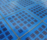
The global production of photovoltaic modules is dominated by the mono and micro-crystalline silicon market with high purity PV-grade Si obtained with the high consumption of energy. Recently, thin film technologies have become an interesting alternative with a higher potential for the reduction of manufacturing costs. Among them, Cu(In,Ga)Se2- (CIGS-) based technologies have demonstrated the highest efficiency, having obtained, in 2011, a record value of 20.3% for a 0.5 cm2 cell that is already comparable to the 25% record in c- Si solar cells.
This fact explains the significant growth in the global industrial CIGS module production from about 150MW/a in 2009 to over 2GW/a in 2011, even if the struggling market situation is forcing many CIGS-based companies into bankruptcy.
Many of the current production methods in CIGS industrial technology typically rely on costly, difficult to control (over large areas) vacuum-based deposition techniques that require very expensive equipment with high initial capital expenditure. In front of this, Scalenano proposes the development and scale-up of alternative non-vacuum processes based on chemical routes that have a higher potential for the reduction of costs, being compatible with their industrial implementation at mass production levels. These include not only processes based on the electrodeposition of nanostructured precursors, but also new processes with very high potential throughput and process rates, as those based on the use of printing techniques with novel nanoparticle ink formulations and new cost-effective deposition techniques. In all of these cases, interest is motivated by the higher potential of these simpler approaches for a more efficient exploitation at industrial mass production level of the cost reduction capabilities of thin film technologies.
Objectives
The Scalenano project involves 13 partners including various research institutes, universities and companies, each of them bringing a high level of experience in different fields for materials synthesis, characterisation or devices fabrication. The achievement of the objectives of Scalenano, which will, in turn, help Europe to regain its competitiveness and leadership in PV technologies, requires the development of a collaborative action at European level that exceeds the funding and infrastructure complementary capabilities that can be obtained with regional, national or even international bilateral co-operative programmes. The employment of a European approach allows us to make use of the strong background and competences available within these groups, and to therefore exploit their complementarities for the consolidation of a competitive European PV industry.
The project has been designed to have actions in each stage of the fabrication of a PV module, from the basic research in materials science to the up scaling of large area modules. A special effort will be made to improve the homogeneity and cell and module efficiency of electro-chemical-based technologies that involve the electrodeposition of nanostructured precursors followed by a recrystallisation step.
New ink formulations and deposition processes for the preparation of highly crystalline quality CIGS absorber layers with very high uniformity will also be investigated. The preparation method for the absorbers will be investigated in depth and optimised, as previous steps for the development of solar cells at laboratory scale. The project also includes the development of scalable non-vacuum based processes for the synthesis of the transparent conducting oxides (TCO).
Strategies
One of the main strategies in Scalenano is the transfer of knowledge from cell to module level. The industrial implementation of concepts for low-cost manufacturing of solar modules with simpler processes is essential. In this way, a huge effort will be focused on the enhancement of large area efficiency of CIGS mini-modules and modules, by the optimisation of different parameters as the Ga insertion in the absorber, the improvement of homogeneity, reducing the processing time, absorber thickness, costs, etc.
The development and implementation of non-destructive methods for process monitoring and characterisation (Raman, PL/EL-based techniques) at both in situ (real-time) and ex situ levels, as in-line and on-line quality control will be a key issue in improving the process yield at the production lines and reducing manufacturing costs. The project also includes the extension of previously developed processes to new alternative photovoltaic materials, such as those based on Indium free kesterites (Cu2ZnSnS4(Se4) compounds) that have already been proposed as medium to long-term alternatives to CIGS.
Scalenano is an ambitious project, and, as such, many challenges will inevitably be encountered. One of the main hurdles will be to increase the efficiency of non-vacuum process-based solar cells with regard to the well-known higher efficiency vacuum processes. It is also expected that the demonstration and improvement of electrodeposition-based processes for their scale-up to industrial level in terms of reproducibility, uniformity, robustness and yield will also prove to be a considerable challenge.
Other important challenges will include the design and implementation of new cell architectures based on nanostructured TCOs (nanowires, nanorod arrays) for higher efficiency devices and their scalability to large areas.